Printing of Nano and Microscale Electronics and Sensors


Commercial nanoelectronics device manufacturing is very expensive, with fabrication facilities costing up to 17 billions and requiring massive quantities of water and power. The cost of the next fabrication in Taiwan is projected to reach $20 billion. Meanwhile, the Internet of Things (IoT) where a network of physical objects embedded with sensors, electronics, software and connectivity has an estimated market of $11 trillion over the next few years. These IoT market projections will be significantly accelerated by the availability of ubiquitous low cost sensors which will be difficult considering the current cost of fabrication.
This new disruptive technology will enable the printing of nanoelectronics at the same scale but at a facility that will cost 100 times less than new conventional facilities. The cost of the printed nanoelectronics will also be 10-100 times less than conventionally fabricated electronics. The new technology, directed assembly-based printing technology, can print circuits 1000 times smaller and1000 time faster than inkjet based or 3D printing. This scalable new technology will also allow device designers to use any organic or inorganic semiconducting, conductive or insulating material on flexible or rigid substrates, including nanomaterials such as 2D, graphene, quantum dots, nanotubes, etc. Printed electronics can significantly lower electronics and sensor costs; however, current commercial printing system can only print 20 micron and larger line width using mostly organic semiconductors.
The new technology is enabled by directed assembly-based nanoscale printing at ambient temperature and pressure that prints faster and smaller (down to 20nm) structures than ink-jet based printing. The technology enables a nano and microscale additive printing platform with heterogeneous integration of interconnected circuit layers (like CMOS) of printed electronics and sensors. This will lower the price of consumer or power electronics by 10-100 times and results in orders of magnitudes lower energy and water consumption.
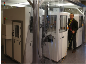
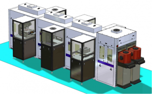
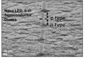
The directed assembly-based printing processes were specifically created to be scalable, sustainable and designed to enable precise and repeatable control of printing of various nanomaterials at high-rate. Using this technology, various nanomaterial based device components such as transistors, sensors, touch display, nano LEDs have been printed including transistors, diodes and inverters using 2d materials, GaN or organic electronics. In 2014, the CHN unveiled the world’s first nanoscale fully automated offset printing system (NanoOPS) prototype with built-in alignment and registration. The second generation was unveiled a few months ago with large substrate and precise nanoscale precise alignment and registration. The technology has been used to print a biosensor platform for real-time pathogen monitoring and for wearable sensors to monitor physiologic state. These printed flexible sensors were printed for wearable sensors that could be used as an electronic skin or for physiological monitoring as well as environmental monitoring. A micro chemical sensor was also printed that is less than one tenth of a millimeter to detect a variety of chemicals in liquid or gas.
How does printing of nanoscale electronics work?
